|
This document is intended
for A-100 users who want to learn a little bit about the technical
details of the A-100. We will start with some electronic basics and
introduce at first the most important electronic parts used in the A-100
circuits. Then we will show how some basic circuits (like attenuators,
amplifiers, mixers, inverters and so on) can be realized with these
parts. The following paragraph will show some simple modifications of
A-100 modules: e.g. changing the sensitivity of CV or audio inputs,
increasing or decreasing output levels (e.g. VCAs or mixers with maximum
amplification > 1), adding offset feature to mixers, changing between
DC and AC coupled inputs/outputs, adding feedback inserts for VC
resonance to all filters and many more.
This page starts September 2004. New items will be added little by
little. If you have any suggestion for this page please send your ideas
to hardware@doepfer.de. We will
try to fulfil all wishes, providing they are possible and will not
contain confidential information.
Additional information about
technical details (e.g. CV/gate control principles, A-100 bus, A-100
power supply) and mechanical details (frontpanel measures, A-100 frame
concept) is available in these documents:
The A-100 service manual is
available only for A-100 customers (see price
list for current price). The words -
mainly building, testing and adjustment notes for the manufacturer - are
in German but the schematics, silk screen and bill of material are
international.
Other pages of interest for
DIY:
|
|
|
|
|
1. Electronic Parts
(For some parts different signs are shown. Normally the left one is used
in USA or Japan, the right one in Germany or Europe)
|
|
|
|
Fixed resistors
A resistor is determinded by
these parameters:
-
value (... Ohm, ...
kOhm, ... MOhm, usual abbreviations kOhm = k and MOhm =M, e.g. 2.2
kOhm = 2.2k or 2k2)
-
power (.. mW, ...W)
-
tolerance (%)
-
max. voltage
-
dimensions (e.g. length,
diameter and especially the grid between the legs on the pc board)
In the A-100 normally only
resistors with 1/4W (250mW) and 5%, 1% or 0.1% tolerance are used. For
the value and tolerance of a resistor normally a color code is used
(should we add the color code at this place ?).
|
|
|


|
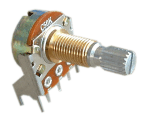
Potentiometers
Potentiometers are available
as rotary potentiometers or fader types. Normally, a potentiometer has 3
terminals: two end terminals and a slider terminal (upper picture). The
slider touches a resistance surface that is located between the end
terminals. Sometimes the second end terminal is not shown (lower
picture) if only one end terminal is required, e.g. if the part works
only as a variable resistor rather than a voltage divider.
A potentiometer is
determined by these parameters:
-
value (... Ohm, ...
kOhm, ... MOhm)
-
power (.. mW, ...W)
-
tolerance (%)
-
characteristics (law)
-
mechanical dimensions
(e.g. diameter, type, length and material of the axis, distance and
diameter of the holes required on the pc board, position of
auxiliary terminals without electronic function and so on)
The characteristics -
sometimes even called law - is a very important parameter of a
potentiometer. This parameter describes the connection between the
rotary angle (resp. fader position for fader potentiometers) and the
resistance value between terminal 1 and slider terminal. Typical
characteristics are linear, logarithmic and inverse logarithmic.
Sometimes special characteristics are used (e.g. S-type law) but these
are not very common. For audio attenuation normally logarithmic
potentiometers are used as the human ear senses the loudness of an audio
signal in a logarithmic way too. The same applies to potentiometers that are
used to control time parameters (e.g. attack/decay/release time of an
envelope generator). For attenuation of control signals normally linear
potentiometers are used. For special functions inverse logarithmic
potentiometers are used (e.g. resonance/emphasis control in filter
circuits).
Another special type is a stereo potentiometer: two potentiometers with
one common axis. The values for the two potentiometers vary in the same
way. Used e.g. for manually controlled filters or stereo applications.
Other special types of potentiometers are not described here (e.g. dual
potentiometers with 2 concentric axis, or potentiometers with additional
terminals) as they are not used in the A-100.
A very special circuit is a
so-called vactrol. This is a combination of a light depending
resistor (LDR) and LED both put into a small 100% light-proof
case. For details please refer to the vactrol
document.
 |
 |
| front view |
rear view |
| Potentiometers
used in the A-100 |
The above pictures shows the
type of potentiometers used in the A-100 system. These potentiometers
are equipped with a mounting bracket that increases the mechanical
stability. For most of the A-100 modules the potentiometers (together
with the sockets) are used to mount the pc boards to the front panels.
The A-100 potentiometers are available as spare parts with these values:
10K (A and B), 50K (A, B and C), 500k (B), 1M (A and B) with A =
logarithmic (audio type), B = linear and C = inverse logarithmic
(ususally for filter resonance controls used). For prices please look at
the price list.
|
|
|

|
Trimming potentiometers
The electronic function of a
"normal" potentiometer and a trimming potentiometer is the
same. The only difference is the mechanical appearance: trimming
potentiometers are normally much smaller and have a very short axis that
is adjusted with a screw driver. Trimming potentiometers are used to
adjust parameters that have to bet set once at the factory and that are
normally not controlled by the user (e.g. offset frequency and scale of
a VCO, maximum/minimum limitation of values, adjustment of click/pop
feedthrough of sound processing devices like VCA, VCF, ring modulator,
frequency shifters and so on). Sometimes users replace trimming
potentiometers with normal ones to have access to such additional
parameters.
Trimming potentiometers are available normally only linear.
Apart from that they are defined by the same parameters as normal
potentiometers.
|
|
|


|
Capacitors
A capacitor is determinded
by these parameters:
-
value (... pF/picofarad,
... nF/nanofarad, ... uF/microfarad, usual abbreviations pF =p, nF
=n, uF =u, 2.2 nF = 2.2n or 2n2)
-
type of dielectric
(foil, ceramic, multilayer, electrolytic)
-
tolerance (%)
-
max. voltage
-
polarized/non polarized
(electrolytic capacitors are normally polarized)
-
dimensions (e.g.
length/width/height or length/diameter and especially the grid
between the legs on the pc board)
In the A-100 all types of
capacitors are used. Value, voltage and tolerance are normally written
as normal characters on the component (e.g. 4n7 63V). But even color
codes and number codes are used (e.g. 103 means 10x1000=10000).
Sometimes it is difficult to find the value of a capacitor. E.g.
"100" without additional pF/nF could mean 100pF or 100nF. Some
experience is required to find out the correct value if the declaration
on the component is not readable, or complete. To be certain of a
capacitors value, one could use a capacitor
measuring instrument such as a multimeter with capacitor measuring
option.
So-called electrolytic
capacitors are used for values of 1uF and more as the other types of
capacitors would be too large. Normally electrolytic capacitors are
polarized (i.e. one has to pay attention to positive and negative
terminal of the part). If there are "+" or "-" signs
in a schematic this means that an electrolytic capacitor is used. The
three examples on the left with "+" and "-"
signs denote an electrolytic capacitor.
Other types of capacitors
(e.g. variable capacitors) are not used in the A-100.
|
|
|


|
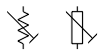
Diodes
Electronic part that works
as one-way for electric current. The triangle terminal (left) of the
symbol is the positive side (or anode), the single vertical line (right)
is the negative terminal (or cathode). Used e.g. for clipping,
rectifying or overvoltage protection. Even light emitting versions (LED)
available in different colors (red, green, yellow, orange, blue, white).
In this case the brightness is approximately proportional to the
current.
A very special circuit is a
so-called vactrol. This is a combination of a light depending
resistor (LDR) and LED both put into a small 100% light-proof
case. For details please refer to the vactrol
document.
|
|
|


|
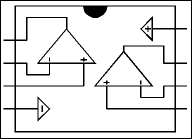
Transistors
Different types of
transistors are available, e.g. bipolar npn or pnp, field effect (FET).
A transistor can be used with the suitable circuit (i.e. with additional
resistors and capacitors) e.g. as amplifier, switch or current source.
|
|
|
|
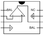
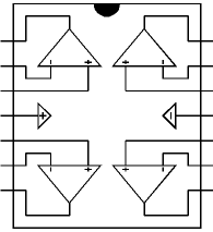
Operational Amplifiers
Operational amplifiers are
special integrated circuits that make available a standard amplifier
with 2 inputs (inverting and non-inverting input) and high amplification
(typ. > 1000). Circuits with one, two or more opamps
(abbreviation for operational amplifier) are available. The following
table shows the pin-out of the most popular types of single, dual and
quad opamps.
 |
Single type
e.g. uA741, TL061, TL071, TL081,
TLC271, NE5534, LF411, LF351, LF356 |
 |
Dual type
e.g. uA747, LM1458, LM4558,
TL062, TL072, TL082, TLC272, NE5532, LF412, LF353 |
 |
Quad type
e.g. LM124, LM224, LM324, TL064,
TL074, TL084, TLC274, LF444 |
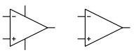
The power supply pins
(marked with the "+" and "-" triangles) of the integrated circuit
in question have to
be connected to +12V and -12V for A-100 applications. In schematics the power
supply pins of opamps are often omitted. The left opamp symbol includes the
power supply pins. The right symbol is without the power supply pins.
Unused OpAmps (if e.g. only 3 devices of a quad opamp are used) have to
be terminated in this way: non-inverting input has to be connected to
GND, inverting input and output have to be connected (directly or even
via resistor in the 1k...100k range).
|
|
|


|
Switches
A lot of different switches
are available. There exist different distinguishing marks,
e.g.:
The pictures show from top
to bottom the symbols for a simple on/off switch (SPDT with one ON
contact only) , a change-over switch (SPDT with two ON contacts), a
rotary switch with 3 positions, a change-over switch with middle
position (SPDT with ON-OFF-ON) and a rotary switch witch 5 positions.
|
|
|

|
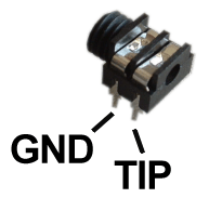
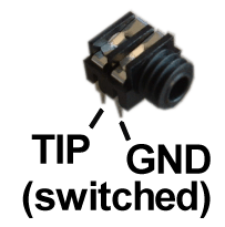
Jack sockets
Standard sockets used in the
A-100 for all inputs and outputs. Provided that a plug is inserted into
the socket the GND and tip terminals of the plug are connected to the
corresponding terminals of the socket. The tip is normally the
"hot" pin, i.e. the terminal leading the CV resp. audio
signal. The sockets are equipped with switching contacts (the arrow in the symbol).
Both the GND and tip terminal are switched but only the switching
feature of the tip terminal is used in some A-100 modules. Provided that no plug is
inserted into the socket the switched tip contact (arrow terminal in the
left symbol) is
connected to the "normal" tip contact (the terminal represented by the
horizontal line in the left symbol). As soon as a plug is inserted this connection is
interrupted and the signal at the tip of the plug is connected to the
tip terminal of the socket. This feature can be used for default connections
(i.e. connection within a module that is established provided that no
plug is inserted into the corresponding socket). Example: internal
default connections of the A-109 signal processor.
This function is often called "normalling" or
"normalizing".
 |
 |
| rear view |
front view |
| jack
sockets used in the A-100 |
The above pictures show the
type of jack sockets used in the A-100 system. For most of the A-100
modules the sockets (together with the potentiometers) are used to mount
the pc boards to the front panels. The A-100 sockets are available as
spare parts. For prices please look at the price
list.
|
|
|
|
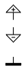
Power Supply
For each circuit, a power
supply is required. The three symbols to the left side denote +12V, -12V and
GND. Some circuits may require no power supply (e.g. multiples or the simple
attenuator below) or only a positive supply. All circuits that use
operational amplifiers require all three +12V, GND and -12V. Some
modules even require +5V (mainly "digital" modules with
digital circuits - like microprocessors, memories, or logic circuits -
which often require a +5V power supply).
|
|
|
2. Basic circuits
|
|
|
|
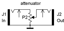
Simple attenuator
This is a simple passive
attenuator (i.e. no power supply required). J1 is the input socket, J2
the output socket. A typical value for P2 is 10k...100k. A linear or
logarithmic type can be used for P2 (logarithmic especially for audio
applications as the loudness characteristics of the human ear is approx.
logarithmic).
|
|
|
|
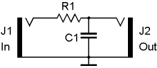
Simple lowpass
This is a simple passive
lowpass with 6dB/octave slope. A non-inverting amplifier can be added at
the output (and even at the input) to make the circuit independent of
input/output impedance (i.e. the "loads" connected to J1 resp.
J2). Replacing of R1 by a vactrol leads to simple voltage controlled
lowpass filter. Replacing R1 by a potentiometer leads to a simple
manually controlled lowpass filter
Frequency of the lowpass: f
= 1/(2 * Pi * R1 * C1) with Pi = 3.14
Example: R1 = 47kOhm, C1 = 10nF -> f ~ 340 Hz
|
|
|
|
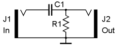
Simple highpass
This is a simple passive
highpass with 6dB/octave slope. A non-inverting amplifier can be added
at the output (and even at the input) to make the circuit independent of
input/output impedance (i.e. the "loads" connected to J1 resp.
J2). Replacing of R1 by a vactrol leads to simple voltage controlled
highpass filter. Replacing R1 by a potentiometer leads to a simple
manually controlled highpass filter
Frequency of the highpass: f
= 1/(2 * Pi * R1 * C1) with Pi = 3.14
Example: R1 = 10k, C1 = 2,2n -> f ~ 7.2 kHz
|
|
|
|
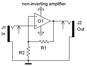
Non-inverting amplifier
This is a simple
non-inverting amplifier: The term "non inverting" means that
the polarity of input and output signal are the same. In other words: a
positive input signal applied to J1 will cause a positive output signal
at J2 and a negative input signal applied to J1 will cause a negative
output signal at J2.
The amplification of this
circuit is 1 + R1/R2.
Example 1: R1 = 0 Ohm (connection), R2 omitted -> A = 1
Example 2: R1 = 47k, R2 = 47k -> A = 2
Example 3: R1 = 100k, R2 = 10k -> A = 11 If
R1 or R2 is replaced by a potentiometer the amplification can be
adjusted. If e.g. R1 in the last example is replaced by a 100k
potentiometer the amplification is adjustable in the range 1...11. This
circuit can be used to built an simple amplifier if the desired audio or
CV signal is too small for a certain application. Attention ! The minimum
amplification of this circuit is 1 (no real attenuation possible
provided that no external attenuator is used).
|
|
|
|
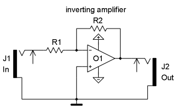
Inverting amplifier
This is a simple inverting
amplifier: The term "inverting" means that the polarity of
input and output signal are opposite. In other words: a positive input
signal applied to J1 will cause a negative output signal at J2 and a
negative input signal applied to J1 will cause a positive output signal
at J2.
The amplification of this
circuit is - R2/R1 (" - " indicates the opposite
polarity of input and output)
Example 1: R1 = R2 = 47k -> A = - 1
Example 2: R1 = 10k, R2 = 100k -> A = - 10
If R2 is replaced by a potentiometer
the amplification can be adjusted. If e.g. R2 in the last example is
replaced by a 100k potentiometer the amplification is adjustable in the
range 0...-10. This circuit can be used to built an simple (inverting !)
amplifier if the desired audio or CV signal is too small for a certain
application.
The minimum amplification of
this circuit is zero (if R2 = 0). To obtain a non-inverted output
another inverting amplifier with amplification - 1 has to be used.
The inverting amplifier can
be extended by adding more input sockets (J1) and corresponding input
resistors (R1). The right terminals of all input resistors are connected
to the inverting input (-) of the operational amplifier O1. The relation
between the corresponding input resistor R1 and R2 (the same for all
inputs) defines the sensitivity of the input in question. If all
resistors have the same value (e.g. 100 kOhm) the amplification is
"1" for all inputs. Lowering R1 (e.g. 47k or 22k) increases the sensitivity of
the input in question. Increasing R2 (e.g. 220k or 1M) increases the amplification resp.
sensitivity for all inputs simultaneously.
The minus terminal of the operational amplifier is often called
"virtual GND" in this circuit as the voltage measured at this
point is very close to GND within a few millivolts - independent of the
incoming voltages! The
first circuit example (chapter 3: "CV mixer with offset
function") shows a typical application of inverting
amplifiers with several inputs.
|
|
|
|
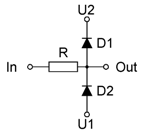
Voltage clamping /
limiting / clipping
This is a circuit that
limits an incoming voltage to the range U1-UD2 ... U2+UD1. The voltage
U1 has to be less than U2. UD1 and UD2 are the forward voltages of the
diodes D1 and D2. To keep these voltages as small as possible Schottky
diodes (e.g. BAT42) ore germanium diodes are recommended because their
forward voltages are in the 0.2...0.3V range. R works as a serial
protection resistor. A typical value for R is 1k.
A typical application is the
limitation of an analog voltage to 0...+5V (e.g. for the inputs of Pocket
Electronic or USB64). In this case U1 is
connected to GND and U2 to +5V. Another
application is sound distortion by voltage clipping. If U1 and U2 are
variable voltages (e.g. outputs of operational amplifiers of one of the
circuits in this document) the clipping levels can be voltage controlled
too.
|
|
|
|
|
3. Circuit examples
|
|
|

|
Mixer with optional
offset function and inverted/non-inverted outputs
Inputs J1 ... J3 are
standard inputs.
Input J4 has offset function provided that no plug is inserted into J4
as the switching contact of J4 is connected to the positive supply
voltage in this case (via the protection resistor R8). At
J5 the inverting sum of all inputs is available. J6 outputs the
non-inverting sum. P5 allows an additional attenuation of the complete
signal (affects only J6).
Typical values for the parts
used:
O1, O2 = LM1458, TL082, NE5532
P1...P4 = 47k linear (CV) or log (audio)
R1...R7 = 100k (for overall amplification 1)
To obtain a higher overall amplification R5 has to be increased (e.g. to
220k for overall amplification ~ 2 or to 1M for overall amplification ~
10).
The value of R8
defines the offset range (about 0...+6V for R8=33k, a lower
value of R8 will increase the offset range and vice versa). |
|
|
|
Matrix Mixer
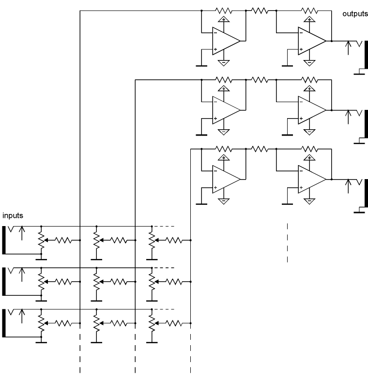
|
Matrix Mixer
The CV mixer described above
can be expanded to a so-called matrix mixer. This circuit has several
inputs available (three in the example circuit) that can be mixed to
different outputs (three in the example circuit) with adjustable levels.
At each point of the matrix a potentiometer is available that defines
the level for the matrix junction in question. The
circuit can be used for CV or audio applications. The number of inputs
and outputs can be increased to the desired value of columns and rows.
For each of the outputs the two OpAmp circuit with the corresponding
output socket is required. For each input another socket and the
corresponding quantity of potentiometers and resistors is required.
Typical values for the parts
used:
All operational amplifiers: LM1458, TL082, NE5532
All potentiometers: 47k linear (CV) or log (audio)
All resistors: 100k
To obtain a higher or smaller overall amplification the feedback
resistor of the first (left) OpAmp of each output circuits has to be
adjusted (as described above).
It is recommended to use a
separate pcb for the output circuits. The input sockets and matrix
potentiometers/ resistors can be wired by hand very easily.
|
|
|
|
Matrix Mixer II

|
Matrix Mixer II
The matrix mixer circuit
described above can be modified to obtain polarizer function for the
controls. This means that zero level appears at the center position,
positive levels appear clockwise from center (addition), negative levels
counterclockwise from center (subtraction). An
(optional) switch is used for each column to select between normal mixer
mode (same function as the matrix mixer above) or polarizer mode for
this column. If a multiple switch is used the complete unit can be
switched between normal or polarizer mode.
The typical values for the parts
used are the same as for the matrix mixer above. But the potentiometers
have to be linear types ! Otherwise the zero position is not the
center position. |
|
|
|
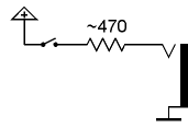
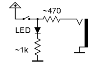
Manual Gate
|
Manual Gate
The left picture shows the
basic circuit of a manual gate. The 470 Ohm resistor serves as a short
circuit protector. Without this resistor the +12V supply would be
shorted to GND if a patch cable is inserted to the socket while
the button is pressed. The
right picture is expanded by a LED display that lights up while the
button is pressed.
|
|
|
|
Or-wired sockets
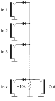
|
Or-wired sockets
The left picture shows the circuit of
"or-wired" sockets. This circuit is useful to combine gate or
trigger signals. The incoming signals are or-wired, i.e. if any of the
inputs is "high" the output turns "high" too
("high" means a positive voltage in the range of typical
+5...+12V). If none of the inputs is high the 10k pull-down resistor
pulls the output to GND, i.e. "low". For most applications
this resistor is not required as the input load of the following module
acts as pull-down resistor. But it should be added to be on the safe
side. As a
modification of this circuit even "and-wired" sockets can be
realized. But this type of combination is not used very often: all
inputs have to be "high" to turn the output to
"high". For all other conditions the output remains
"low". On this the diodes have to be flipped (i.e. the
cathodes at connected to the input sockets) and the resistor has to be
connected between the output and +12V (so-called pull-up resistor). In
addition the switching contacts of the input sockets have to be
connected to GND (normalled to GND). This measure is necessary in order
that unused sockets read "low". Otherwise unused sockets would
read "high" because of the pull-up resistor. For
example a multiple A-180 can be modified with 7 additional diodes and
one resistor to obtain seven or-wired sockets and one output socket. For
this the pcb tracks between the eight multiple sockets have to be
interrupted (not the GND connections, only the "hot"
connections) and re-wired with the diodes and the resistor.
|
|
|
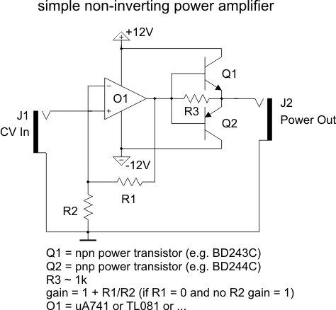 |
Non-inverting power amplifier
This is a simple non-inverting
power amplifier that can be used to drive loads like light bulbs,
LED bars, fairy lights, motors, magnets, relays or other loads.
Pay attention that the connected load is suitable for 12V supply
voltage. Otherwise the supply voltages of the operational
amplifier and the power transistors have to be adapted. If only
positive output voltages are required Q2 can be omitted. If an
operational amplifier is available in the preceding module (e.g. a
mixer A-138) this operational amplifier can be used and only Q1,
Q2 and R3 have to be added. The maximum output current depends
upon the specifications of the power transistors. Pay attention
that the power supply has to be able to deliver the additional
load current ! For higher currents (~ beyond 100mA) the
transistors have to be mounted on suitable heat sinks. Attention:
The output is not short circuit protected. If a standard
A-100 jack socket is used the output connection has to be
established before power is turned on ! During the
insertion of a plug into the jack socket a short circuit is made
for a short time. Therefore another type of socket is recommended
for the output (not the jack socket shown in the picture).
If only positive voltages
referenced to GND are required (e.g. to drive lamps, LEDs, motors and so
on) the circuit becomes very simple: In this case only Q1 is required
and R3 can be omitted (i.e. the base of Q1 is connected to the output of
the OpAmp, the collector of Q1 goes to +12V and the emitter is the new
"power output" - this circuit is called "emitter
follower"). This circuit can be used with all module outputs. In
our A-100 demo system an A-183-2
Offset Generator/Attenuator/Polarizer, that has been modified in this
way (i.e. only Q1 = BD243C), is used to drive a LED strip that is glued
by means of a double sided self-adhesive tape to the upper front rail of
the case. The brightness of the LEDs can be controlled manually and/or
by a control voltage (e.g. an ADSR which is is sync with a running
sequence). A picture of the A-183-2 with LED strip will follow
soon. |
|
|
|
4. Module
modifications
|
|
4.1. General modifications (not
for one module only)
|
|
4.1.1. Changing the sensitivity of manual
controls, control voltage inputs and audio inputs
|
|
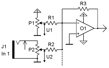
The following picture shows the control
voltage input circuit for most of the A-100 modules:
|
|
P1 is the manual control of
the corresponding parameter (e.g. tune for a VCO, frequency for a VCF,
manual gain for a VCA, manual phase shift for a phaser and so on). P1
generates the voltage U1.
J1 is the (first) input socket for the external control voltage. P2 is
the corresponding attenuator. The slider of P2 outputs the voltage U2.
Additional CV inputs with our without attenuators may be available (e.g.
two or more CV inputs for frequency control for a VCF). The dashed line
in the picture is the common point in the circuit where all CV's are
added.
The output voltage of the circuit (output of O1) is used to control the
corresponding parameter (tune, filter frequency, gain ...) of the module
in question. The output voltage is defined by:
R3/R1 * U1 + R3/R2 * U2
The relations R3/R1 resp.
R3/R2 determine the sensitivity of the corresponding control (P1) resp.
input (J1/P2). If for example all resistors are 47k (a common value in
the A-100) the sensitivity is 1 for each input. Provided that R3 remains
unchanged the resistors R1 and R2 determine the sensitivity of the
corresponding control resp. input. Reducing the resistance of R1 resp.
R2 increases the sensitivity of the manual control (P1) resp. input
(J1/P2). Increasing the resistance of R1 resp. R2 reduces the
sensitivity. To modify the
sensitivity of a control knob (P1) or CV input (J1/P2) the corresponding
resistor R1 resp. R2 simply has to be changed.
Changing the resistance of R3 has the opposite effect and affects the
sensivity of both the manual control and CV input.
|
|
The audio input circuit for most A-100
modules is similar but the manual control P1 is absent (a DC offset
would not make sense for an audio input, audio signals are AC signals).
Normally only one audio input is available but there are exceptions
(e.g. VCA A-130 and A-131, signal processor A-109). To change the
sensitivity of an audio input simply the resistor R2 connected to the
slider P2 of the audio input has to be replace. A smaller value will
increase the sensitivity and consequently lead to clipping/distortion
for higher input levels. Especially for the first A-100 VCFs and VCAs
(A-120, A-121, A-122 and first versions of A-130, A-131) the
audio inputs have been designed to avoid distortion with standard A-100
signals (e.g. VCO). Lowering the input resistors will allow distortion
for these moduls too.
Even the input resistors of CV or audio
mixers (e.g. A-138a/b) can be changed to allow "real"
amplification (i.e. > 1). The factory values of the resistors in the
mixer modules A-138a/b allow a maximum amplification of about 1 (which
is not really amplification). Reducing the input resistors (R2 type) or
increasing the feedback resistor (R3 type) will increase the
amplification of the circuit.
The factory values of the corresponding
resistors (R1, R2, R3) for all modules can be found in the A-100 service manual.
Normally they are in the 100k range (~ 47k...220k).
|
|
|
|
4.1.2. Insert sockets for external
resonance control of filters, phasers and similar modules
|
|
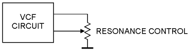
To enable voltage control of resonance for
filters insert sockets in the feedback loop can be used.
|
|
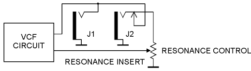
The left picture shows the
resonance control in a filter or phaser circuit. Essentially it is an
attenuator that controls the feedback of the circuit. To enable external
control of the resonance external access to the feedback loop is
recessary.
For resonance control normally C-law potentiometers are used (i.e.
inverse logarithmic, e.g. 47kC).
|
|
|
|
|
This is the first solution
how to install the insert sockets (pre resonance control). J1 is
connected to the slider of the resonance control. Provided that no plug
is inserted into J2 the function of the module is unchanged as the
switching contact of J2 is active. As
soon as a plug is inserted into J2 the default connection is interrupted
and the signal fed to J2 is used as feedback signal. Consequently J1 and
J2 can be used to insert e.g. an external VCA to control the resonance.
J1 has to be connected to the audio input of the VCA, J2 to the audio
output of the VCA. The resonance control can be used to adjust the
maximum resonance available with different gain settings of the external
VCA. But not only a VCA but any audio processing module can be inserted
into the feedback loop (e.g. phaser, spring reverb, waveshaper, limiter, wave
multiplier, divider, ring modulator, frequency shifter, or even another
filter).
|
|
|
|
|
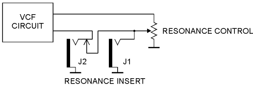
This is another solution how
to install the insert sockets (post resonance control). The
location of the resonance control at the pc board for all modules in
question can be found in the A-100 service manual.
|
|
|
4.1.3. Changing between AC and DC coupling
|
There are two types of coupling between
electronic circuits:
-
AC coupling (alternate current)
-
DC (direct current)
AC coupling means that only the AC
parts of the signal will pass. For this normally a capacitor is used
that connects the two circuits. The minimum value of the capacitor
depends upon the lowest frequency (f) that has to be transmitted and the
input/output impedance (R) of the two circuits. The approximate formula
for the minimum capacity is C ~ 1/(R*f) with f = lowest frequency, R =
in/output resistance
Example: minimum frequency = 50Hz,
in/output resistance = 10kOhm -> C ~ 2 uF (u = micro = 1/1000000). A
usual value would be 2.2uF in this example.
AC coupling is normally used for audio
signals. For audio signals AC coupling has the advantage that unwanted
DC shares in the signal are removed. For some AC processing circuits
(e.g. amplifiers, filters) DC voltages are not allowed in the input
signal. Therefore very often a capacitor can be found in the input stage
of such circuits.
DC coupling means that both DC and
AC parts of a signal are transmitted. For control voltages (normally)
only DC coupling can be used as even fixed voltages (e.g. coming from a
manual control) have to be transmitted.
In a module patch each A-100 module can
be treated as an electronic circuit that is connected to another one.
Consequently one has to take into consideration the type of coupling (AC
or DC) between modules as the strict differentiation
between AC and DC applications os softened for some A-100 modules. E.g.
a VCA can be used to process audio signals (i.e. normally AC coupled
signals) as well as slowly changing CV voltages (e.g. envelope or
modulation amount). Therefore one needs to know if a VCA used is AC or
DC coupled. Another example is a divider (e.g. A-115
or A-163) as even these module can be used to
process audio or (slow) clock/gate signals.
|
|
Luckily it is not very
complicated to switch between AC and DC coupling. All one has to do is
to bride (i.e. short circuit) the capacitor in case of an AC coupled
in/output. The left picture shows how
the switch is connected in parallel to the AC coupling capacitor (the
broken line resistor symbol represents the load to GND that is always
available in each circuit as reference to GND). If AC coupling is
required for a DC coupled in/output simply a capacitor has to be added. From
the schematics it can be seen if an in/output is AC or DC coupled. We
will add this information also to the user's manual for modules that may
be used for both types of coupling. For
some circuits resp. modules changing from AC to DC coupling is not
possible. E.g. the "old" VCAs A-130 and A-131 (those with
CEM3381 or CEM3382) are AC coupled as the special CEM circuits cannot be
DC coupled because of the internal negative reference voltage. The
"new" VCAs A-130 and A-131 (those with CA3080) are DC coupled
and can be used to process CV signals too. A
list with the type of coupling for all modules in question will follow
soon. For most of the modules the question about the type of coupling does
not arise. E.g. all filters are AC coupled and all CV generating and
processing modules (e.g. ADSR, LFO, slew limiter, Theremin, Ribbon
controller, random voltage) are DC coupled. But for other modules the
type of coupling is not obvious (e.g. VCA, divider, waveshaper).
|
|
|
4.1.4. Subsequent bus normalling of modules
|
Only a few modules (typically VCOs, envelope
generators or Midi interfaces) feature access to the CV and Gate signal of the A-100
bus. For details please refer to the information about the module in
question. General information about the CV and Gate signals of the bus
are available in the A-100
FAQ section.
If another module has to be modified accordingly.
Examples:
- rectangle output of an LFO to
"write" the LFO rectangle as gate signal to the bus gate
- gate input of the A-143-2 Quad ADSR from the bus gate
- CV input of a filter from the bus CV
|
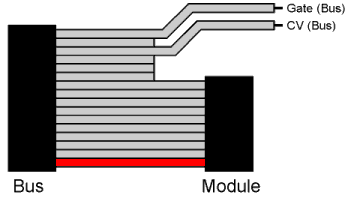
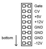 |
The left picture shows the pin out
of the bus. The signals Gate and CV are available at the two
upper pin pairs of the bus (left and right pins are always
connected on the bus board and carry the same signal).
One has to distinguish between
two types of modules (the bus connector is always 16 pin):
- modules with 16 pin male bus
connectors
- modules with 10 pin male bus
connectors
If the module in question is
equipped with a 16 pin male connector both signals CV and gate
are available at the upper two pin pairs of the modules bus
connector. One simply has to wire the corresponding pin (one of
the upper pair for Gate, one of the second pair for CV) of the
16 pin connector to signal in question (e.g. to the rectangle
output of a LFO or to the gate input of an VCADSR or VC Decay).
|
|
 |
|
If the module in question is
equipped with a 10 pin male connector the signals CV and gate
are not available at the modules bus connector. In this case a
special bus cable has to be used. The left picture shows how
this works. A 16 pin ribbon cable with a 16 pin female connector
on one side and a 10 pin female connector on the second side is
used. The 10 pin female connector is used to establish the
connection between the module and the bus. It is put to the
module's 10 pin male connector. The wire of the 16 pin ribbon
cable that corresponds to Gate resp.CV of the bus is connected
to the corresponding input (e.g. gate in, CV in) or output (e.g.
rectangle out) of the module. The wires #15 or #16 are gate, the
wires #13 or #14 are CV. The red marked wire is the bottom wire
that leads -12V (same for all modules).
Pay
attention that only one module is allowed to "write"
to the same bus signal. If two or more modules write
to the bus this leads to a short circuit of the corresponding
outputs.
The bus board has available two
jumpers (located in the middle of the bus board). If these are
removed the gate and CV lines are divided and both the left and
right part of the bus board are separate bus areas concerning CV
and gate. The power supply lines (-12V, GND, +12V, +5V) are
always connected and cannot be interrupted.
If more than three VCO CV inputs
are connected to the same bus the Bus
Access Module A-185 is recommended to write to the bus.
Otherwise signal losses may occur and lead to scaling problems. |
|
|
|
|
|
4.1.5. Subsequent socket normalling of modules
|
|
coming soon ....
(how to make use of unused switching
contacts of sockets for module pre-patching)
|
|
4.2. Specific modifications for
certain modules
Important note: Warranty
is void if these modifications are carried out by the customer !
|
|
4.2.1. A-128 filter bank modification: single outputs
|
|
This document shows how to add single
outputs to the filter bank A-128: A128_single_outputs.pdf
|
|
|
4.2.2.
A-136 Modification: bypassing the internal pre-amplifier
|
Module A-136
contains an internal pre-amplifier that is used to amplify the input
signal by about 3.5 before it is processed by the A-136. Especially for
low level audio signals (e.g. output from a VCF) this is useful. But for
all signals with a level beyond ~ 7V this causes clipping before the
internal processing takes place. Especially for the processing of LFOs
or unfiltered VCOs this may cause a problem. To bypass the internal
pre-amplifier resistor R2 has to be removed (e.g. by
pinching off). R2 is the resistor in the upper third of the pcb which is
very close to the rear edge. When R2 is removed the amplification of the
internal pre-amplifier becomes "1" (which means that it does
no longer amplify).
In addition one has to pay
attention that the knob positions may vary a bit from the front panel
printing because of mechanical tolerances of the potentiometers and
knobs (i.e. "0" is not always exactly the neutral
position for "A", "+A" or "-A")
|
|
|
4.2.4. A-151 Modification: switch for
limiting the number of steps (only for old versions of A-151)
|
A toggle switch 1-0-1 type is required (i.e. with center
position). A hole for the additional switch can be drilled e.g. below
the socket I/O4.
This is how the switch has to be wired:
- terminal 1 to CD4052 pin 11 (= LED control for I/O 2)
- center terminal to reset input via a standard diode (e.g. 1N4148),
cathode (-) on reset, anode (+) on switch terminal
- terminal 2 to CD4052 pin 15 (= LED control for I/O 3)
The new version of the A-151 is already
equipped with this switch. Thank's to Peter Grenader for this idea.
|
|
|
4.2.5. A-148 Modification (old version):
T&H instead
of S&H
|
|
The new version of the Dual S&H module
A-148 has a jumper available for each sub-unit that is used to set the
operation mode for the corresponding sub-unit to S&H or T&H. The
old version of the A-148 was fixed to the S&H mode. To make
available T&H for the old version of the A-148 one has to replace
the capacitor C1 (10nF) by a resistor (about 1k). C1 is available twice
on the pc board: one for the upper and one for the lower unit. It is
also possible to add a switch that is used to switch between S&H
(capacitor) and T&H (resistor).
|
|
|
4.2.6. A-152 Modification: S&H instead
of T&H
|
Normally the eight S&H outputs of the
module A-152 work not as S&H but as T&H outputs (details can be
found in the A-152 user's manual). To obtain S&H function instead of
the T&H function the module has to be modified in that way:
A connection has to be made between pin 6 of the microcontroller IC1 (on
board A, PIC16F676) and pin 2 of IC6 (on board B, DG408). The 10k
resistor R32 next to C5 on board B has to be removed. And that's how it
works: the enable pin of the multiplexer DG408 is normally connected to
+12V ("high") via resistor R32. Pin 6 of the microcontroller
(RC4) outputs a short high pulse whenever the address changes. If the
enable pin of the multiplexer (DG408) is connected to this pin (instead
to +12V via R32) the T&H function changes to a S&H function as
the multiplexer is enabled only for a short time at each address change.
Even a toggle switch that selects the
desired mode can be connected to the pins and the resistor.
|
|
|
4.2.7. A-155 modifications/undo
modifications: gate reset, manual step debouncing
|
|
This document shows how to modify or undo
the modifications of the sequencer module A-155: A155_Modifications_Undo.pdf
There are two possible modifications:
Modification #1 refers to the behaviour
of the gate row. Without this modification the gate output remains
"high" if the sequence stops at a position with the
corresponding gate switch in the on position. If this modification is
carried out the gate outputs turns "low" as soon as the
sequence stops. It's an AND wiring of the gate outpout with the
start/stop state of the A-155. If the A-155 is combined with the A-154
this modification has to be removed ! Modification
#2 is a debounding circuit to avoid multiple triggering if the manual
step button is used. This modification limits the maximal clock
frequency to some hundred Hz (digital low pass). For normal sequencer
applications this is no restriction but if the A-155 is
used e.g. as a graphic VCO the modification has to be removed. It is not
necessary to remove this modification if the A-155 is combined
with the A-154.
|
|
|
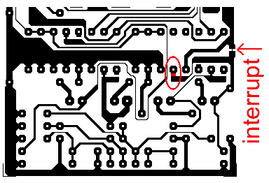
4.2.8. A-155 Modification: changing gate
row into trigger row #4
|
The factory setting of
the function of row #4 of the trigger board is Gate. If
one prefers another Trigger row the following modification
has to be carried out:
The connection marked by the arrow in the picture has to be interrupted.
Instead of this a connection between pin 5 of IC2 (CD4053) and the
close-by pcb track has to be installed (solder jumper).
|
|
4.2.9. A-155 Modification: adding
sockets for address outputs
|
|
This is the pinout of the internal 10 pin
connector that leads from the small control board to the potentiometer
and switch boards:
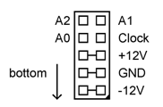
Besides the supply terminals (-12V, GND,
+12V) these signals are available:
- Address signals A0, A1, A2
- Clock signal
The A-155 control board includes a simply
binary counter (CD4024) that generates the address signals (A0, A1, A2).
The advance of the binary counter to the next address is triggered by
the clock signal. The control boards outputs the three address signals
and the clock signal. The potentiometer and switch boards receive these
signals. The signals have CMOS levels (~ 0/+12V) as the CMOS circuits of
the control board are 12V powered. They are not TTL compatible ! A
simple solution to have the address signals A0, A1 and A2 and the
internal clock signal available for other modules the corresponding pins
of the control board can be connected to sockets via protection
resistors (typ. 1k). A better solution is to insert suitable buffers
into the outputs. It's also possible to feed the potentiometer and
switch boards with other address and clock signals than those coming
from the A-155 control board. The signals have to be 12V CMOS compatible
(i.e. low = 0V, high = +12V).
All modifications should be carried out by experts only as the modules
contain charge sensitive devices. We have to point out that warranty is
lost if such modifications are carried out.
|
|
|
4.2.10. Modifying the A-124 Wasp Filter
for self-oscillation
|
|
Soldering a 10k resistor in parallel to R13
(27k) leads to self-oscillation of the filter at the max. resonance
setting of the resonance control. R13 is located in the gap between IC1
(CD4069) and IC2 (i.e. the upper CA3080, close to C4/100pF).
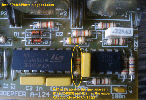
(Thanks to Pierre
Serné for the permission to publish this picture)
|
|
|
4.2.11. Modifying the A-163 voltage
controlled frequency divider for DC coupling
|
|
Shortening the electrolytic capacitor C7
(2u2) changes the output from AC to DC coupling. C7 is located between
the input and the output socket After this modification the A-163 can be
used e.g. for frequency dividing of LFO signals too (only suitable for
rectangles). Instead of the short circuit even a switch can be used that
switches between AC and DC coupling. The only difference between AC and
DC coupling is that in the DC coupled mode the output rectangle switches
from GND to ~ +5V while in the AC coupled mode the signal is
symmetrically around GND (~ -2.5/+2.5V). Usually even the DC coupled
mode can be used for audio signals as most of the audio processing
modules (e.g. filters) have an AC coupled audio input that removes the
positive offset of the A-163 output in DC coupled mode.
|
|
|
4.2.12. Modifying the A-165 trigger
inverter/modifier for S-Trig input
|
|
This document shows how to modify the
trigger modifier/inverter for S-Trig input: A165_strig_modification.pdf.
The modification is very simple. Just one 100k resistor has to be added
between the input socket and +12V.
|
|
|
4.2.13. Shortening the output protection
resistor of A-156, A-170 and other modules
|
Most of the A-100 modules are equipped with
a 1k protection resistor at the output. This resistor protects the
output of the module against shortening to GND or shortening to another
output. In sensitive CV applications (typically driving the CV input of
one or more VCOs) these protection resistors may cause a small voltage
drop that leads to inaccuracy in the 1V/Oct scale. There are two
solutions:
- Usage of a CV buffer between the
output of the A-156/A-170 and the VCO input(s), e.g. A-185-1
or A-185-2)
- Shortening the output protection
resistor
If the protection resistor is shortened
the output is no longer protected against shortening to GND or another
output but the voltage drop caused by the protection resistor is
eliminated. For the A-170 the protection resistor is R2 (positioned
below the imprint "A-100 MODULAR SYSTEM" on the pc board. For
the A-156 the resistors are R17 and R20 (above and below the upper
integrated circuit IC3/TLC274).
|
|
|
4.2.14. Removing the springs of the A-174
joystick module
|
|
Method #1: Bend very carefully the four metallic
tongues of the corresponding potentiometer that hold the end plate of
the potentiometer in question. E.g. a small screw driver could be used.
Pay attention not to break off the tongues. Then the end plate and the
spring can be removed. Re-install the end plate by bending back the four
tongues. This can be done for both or only one of the two potentiometers
of the joystick.
Method #2:Another possibilitly is to compress the two ends of
the spring and cut with a suitable small cutting pliers without
dismantling the potentiometer. In this case the remnant of the spring
remains in the potentiometer.
Pay attention that warranty is lost if the
joystick is modified !
|
|
|
4.2.15. Meaning of the pin headers of the
A-174-2 wheel module
|
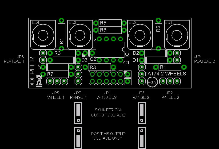
The jumpers JP4 and JP6
are used to install a small voltage plateau around 0V. The plateau
appears if the corresponding jumper is removed (normally used for the
spring loaded wheel only to obtain 0V output in the neutral position).
The jumpers JP3 and JP7 are used to select the output voltage range
(i.e. symmetrical or positive voltage only). Pay attention that this
corresponds to the mechanical adjustment of the wheels ! This means one
has to re-adjust the wheels also if the jumper settings of JP3 or JP7
are changed. That's a bit tricky and only recommended for experienced
users. Otherwise the voltage range of the outputs will be not correct
(e.g. not starting with 0V or a large "dead range" for the
wheel without spring, or not 0V in the center position of the spring
loaded wheel).
Pay attention that
a re-adjustment of the wheels liable to pay costs if the
wheel adjustment has been changed by the customer !
|
|
4.2.16. Changing the BBD circuit in the
A-188-1 BBD module / Adjustment of the A-188-1 BBD module
|
|
The following document
describes the A-188-1 adjustment procedure: A1881_adjustment.pdf
|
|
|
to be continued
|
|
|
5. Simple DIY modules
/ frames
|
|
5.1. Attenuator
|
|
|
This is the simple
attenuator circuit mentioned in chapter 2. The two sockets J1 and J2,
and the potentiometer P2 can be mounted on a blind panel with 8 HP (4 HP
will be a little to small for the potentiometer). To take advantage of
the whole 8 HP panel a second attenuator or a small multiple (i.e. some
connected sockets) can be mounted on the same panel. A value of 50k is
recommended for P2 (linear for CV applications, log for audio
applications).
|
|
5.2. Bypass / Bypass with attenuator
|
|
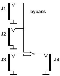
The left circuit is a simple
bypass that can be used to decide if an audio processing module (e.g. a
filter or a phaser) is active or not. J1 and J2 form a miniature
multiple. J1 is connected to the audio source (e.g. a VCO output or a
mixer output), J2 to the audio input of the audio processing module
(e.g. filter). J3 is connected to the audio output of the processing
module. The position of the switch determines if the audio processing
module is active (lower position of the switch) or not (upper position
of the switch). The four sockets and the switch can be mounted on a
blind panel with 4 HP. In
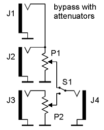
the right circuit the bypass is expanded by two attenuators (P1, P2)
that can be used to compensate possible audio level differences, i.e. no
or little audio level changes appear when the switch is operated. One of
the attenuators may be omitted if not both levels have to be adjusted.
The four sockets, the two potentiometers and the switch can be mounted
on a blind panel with 8 HP. 50k log is recommended for P1 and P2.
|
|
|
|
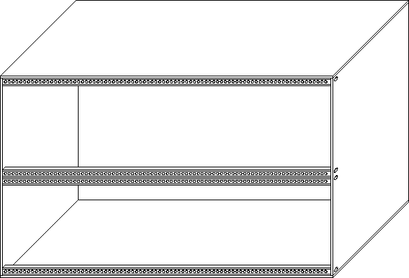
5.3. Self-construction
of A-100 frames
|
|
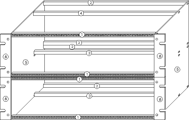
The left picture shows the
construction of the standard 6 HU A-100 frame (A-100G6). The
construction is described in detail in this document:
The standard 6 HU frame is
made of the following components:
-
(1) front rail version 1 (with lip), with threaded inserts (for
module mounting)
-
(2) front rail version 1 (with lip), with slide nuts (for rear
covers mounting)
-
(3) front rail version 2 (without lip), with slide nuts (for bus
board mounting)
-
(4) front rail version 2 (without lip), for increasing stability
only
-
(5) side plate
-
(6) 19" mounting flange
-
(x) top and bottom cover
(not shown in the picture)
A detailed description of
the A-100 frame construction is available as pdf document A100G6_e.pdf The
most expensive parts of the frame are the side plates, mounting flanges
and top/bottom covers. If you do not care much for a 19" compatible
housing a low cost version of an A-100 frame can be built according to
the following instructions. Pay attention that this is suitable for qualified personnel only who are able to
ensure the electrical safety of the final construction. On no
account beginners or laymans are allowed to assemble frames. Dangerous
mains voltage 115V / 230V. Danger to life !
|
|
|
|
|
From the parts list above
only the front rails version 1 with "lip" and threaded inserts
(1) and the accessory screws are required (the screws that are used to
mount the rails to the side plates in the standard version of the
frame). Around these 4 rails a suitable case has to be constructed as
outlined in the left picture. The rails and accessories are available from the
German company ProMA (www.proma-technologie.de)
but there are many other companies on the market too. Even rails longer
than the 19" standard can be used to obtain bigger non-19"
frames (from ProMA e.g. rails with 1m length are available). At
the rear of the case the A-100 power supply (A-100NT12 or A-100PSU2,
with mains inlet, power switch and fuse holder) and the bus boards have
to be mounted with distance sleeves or spacers. The wiring of the power supply and the bus boards is described in
this document:
As these works affects parts, pc boards and cables that conduct mains voltage
(230/115V) carrying out of these works is allowed only for experts or authorized
personnel who are familiar with all valid safety rules. Laymen are not
allowed to carry out these works ! Danger to Life.
|
|
6. Miscellaneous
|
|
6.1. A-100 Power Supply
|
|
The A-100 requires a bipolar/symmetrical
power supply with -12V, GND and +12V. A high quality linear
power supply is recommended. Switching power supplies are not
recommended. We tried several switching power supplies for A-100. The
main advantages of switching power supplies would be the wide range AC
input (typ. 90-240V AC, i.e. no supply modification if you move e.g.
from USA to Europe and vice versa), low price and small shape/weight. As
some customers suggested switching supplies we ordered three types of
switching supplies with different power (Meanwell, Sun Power, Condor/SL)
and installed them into standard 6U/84HP cases and a 12U/168HP monster
case. For all tested supplies the results are very poor. The main
problem is the unsufficient load regulation that may lead to VCO tuning
problems. We found up to 200 mV (=0.2 V) voltage change of the +/-12V
supplies while the load changes. Such load changes are caused e.g. by
different LED illuminations (normally a module will consume more current
if a LEDs is bright compared to the dark state) or other effects (e.g.
frequency changes of VCO/VCF). If the linear A-100PSU2 was used the
+/-12V changed only by about 5mV under the same conditions. Consequently
switching power supplies can be recommended only for
"non-critical" DIY applications (e.g. if only CV
sources/modifiers and audio modifiers are installed). For frames that
include one or more VCOs we recommend the A-100PSU2 or another linear
supply with good load regulation (10 mV or better).
|
|